In late September 2026, Yole Developpement released the "Status of the CMOS Image Sensor Industry 2026" report, while The Business Research Company published an automotive camera module market report on September 29 projecting 10.4% CAGR growth to USD 14.57 billion by 2030. Both reports converge on one conclusion: CMOS image sensors (CIS) are shifting from a volume-driven to a value-driven growth model, with 3D stacked architecture, metasurfaces, and event-based sensors accelerating toward commercialization, while the AI boom compresses advanced stacked-CIS wafer capacity. For overseas OEM/ODM buyers and hardware engineers, this means camera module selection logic is changing fundamentally: continuing to compare prices by megapixel count will systematically underprice architectural value, lock the supply chain, and trigger mass-production delays. This article breaks down the five most common selection pitfalls overseas buyers face in this CIS architecture upgrade wave, with engineering-grade remedies.
Definition first: a CMOS image sensor (CIS) is the semiconductor chip that converts light into electrical signals, the core photosensitive element of any camera module. For the past decade, CIS market growth was driven primarily by shipment volume, fueled by multi-camera smartphone adoption, security-camera deployment, and automotive camera standardization. But Yole reports that global CIS revenue reached a record USD 25.3 billion in 2025, with 2026 returning to normalization, and the industry shifting from volume-driven to value-driven growth, where value is created by rising average selling prices (ASP) rather than shipment growth.
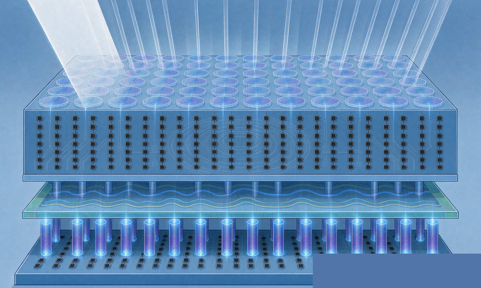
The ASP uplift comes from architectural upgrades. Back-side illumination (BSI) hybrid stacking is now mainstream; Sony's three-layer stacking in iPhone and OPPO sets a benchmark; the industry's focus has shifted from shrinking pixel size to 3D integration, stacking the photodiode layer, logic circuitry (28/22nm), and memory tiers together for lower power, faster readout, and on-chip AI inference. Meanwhile, metasurfaces have moved from lab to production: Apple's iPhone 17 Face ID module and Samsung's beam-splitting metasurface for Xiaomi Civi 5 Pro are both commercialized. Event-based sensors, SPAD (single-photon avalanche diode) arrays, and short-wave infrared (SWIR) imaging are gaining traction in robotics, XR, and low-light applications.
A second variable is the AI industry boom. Yole warns that surging HBM and DRAM demand is tilting wafer capacity toward memory production, compressing stacked-CIS supply, with some smaller CIS makers forced onto 8-inch wafer lines. This means advanced stacked-CIS capacity competition is extending from automotive-versus-industrial into AI-memory-versus-CIS. Under this new logic, buyers still stuck in the old "pick a megapixel count" mindset will fall into at least the following five pitfalls.
Why it is a pitfall: Most buyers carry over smartphone-era selection inertia, treating megapixel count and pixel pitch as the primary CIS selection metrics and comparing prices along those two parameters, naturally gravitating toward the lowest quote with similar specs.
Where the trap lies: The core value of a stacked CIS is not resolution at all. It separates the photodiode layer from the logic layer, maximizing the light-sensitive area while integrating readout circuitry, signal processing, and even AI accelerators on the logic tier. Its real value lies in higher readout frame rates (enabling multi-frame HDR fusion), lower rolling-shutter distortion, on-chip scene classification (offloading the main processor to extend battery life), and larger full-well capacity (boosting dynamic range). Comparing prices by megapixel count is using a resolution ruler to measure a readout-speed-plus-processing product, systematically underpricing the stacked architecture and ending up with a part that looks good on a spec sheet but underperforms in real imaging.
How to fix it: Upgrade the selection metric from "megapixels plus pixel pitch" to a four-dimensional matrix: readout frame rate (does it support the target HDR multi-frame cadence), on-chip processing capability (NPU/AI accelerator, how much main-processor load it offloads), full-well capacity and quantum efficiency (determining dynamic range and low-light performance), and power budget (a critical constraint in mobile and automotive). Keep megapixels as a baseline item, not the comparison axis.
Why it is a pitfall: Metasurfaces sound like a futuristic lab technology, so many buyers assume mass production is years away, do not actively evaluate them during selection, and passively accept whatever the module vendor recommends.
Where the trap lies: Metasurfaces have already entered commercialization. They manipulate light with sub-wavelength nanostructures, achieving the function of a traditional lens group on a single flat element, shrinking module volume while improving optical efficiency and sensitivity. The problem is that the metasurface lens production supply chain is extremely narrow, dominated by a few IDMs like Sony and Samsung, with almost no second-source suppliers offering automotive- or industrial-grade metasurface lenses. Once a product definition specifies a metasurface solution, switching suppliers or building a second source is nearly impossible, the supply chain is locked, and pricing and lead-time leverage is handed to the primary vendor.
How to fix it: Run a metasurface necessity assessment early in selection. Ask three questions: do you truly need extreme miniaturization; can a traditional aspheric glass/plastic hybrid lens meet the optical spec; is the volume benefit worth the single-source risk. If not necessary, prioritize mature aspheric lens solutions. If a metasurface is required, lock the primary supplier while demanding open optical parameter interfaces (focal length, F-number, MTF, transmittance) and pre-stocking a parameter-compatible traditional lens as a downgrade fallback.
Why it is a pitfall: Yole lists event-based sensors, SPAD arrays, and SWIR imaging as emerging sensing technologies "gaining attention," and many engineering teams read such phrasing and rush to adopt them in mass-production projects for differentiation.
Where the trap lies: "Gaining attention" refers to R&D and early-application heat, not production readiness. Event sensors output pixel-level brightness-change events rather than full frames, requiring a completely different neuromorphic vision algorithm stack with scarce development resources. SPAD arrays have low-light single-photon detection potential, but array scale, dark count, and mass-production yield are still climbing. Test standards are immature, existing industrial standards like EMVA 1288 are designed for traditional frame-based CIS, and parameter definitions and certification methods for event sensors and SPAD are still being drafted. Rushing them into mass production risks a triple bind: algorithm delivery delays, yield shortfalls, and unobtainable third-party certification.
How to fix it: Manage emerging sensing technologies on two tracks: R&D preview and mass-production projects. R&D can invest to accumulate algorithm and testing experience; mass-production projects should stick to mature BSI or stacked CIS with complete supply chains, algorithm ecosystems, and certification systems. For event sensors and SPAD, run small-batch validation projects first, and consider mass-production import only after CPK data stabilizes, the algorithm ecosystem matures, and EMVA and other standards cover them.
Why it is a pitfall: After the 2021-2022 chip shortage, many buyers assume CIS capacity has loosened and treat stacked CIS as a standard commodity bought on demand, negotiating only price in contracts without locking capacity.
Where the trap lies: Yole explicitly states that the AI boom is driving HBM and DRAM demand, tilting wafer capacity toward memory production and compressing stacked-CIS supply. Stacked CIS depends on advanced-process logic tiers (28/22nm) and competes with memory and AI accelerators for the same advanced wafer capacity, making its supply elasticity far lower than traditional BSI. When capacity tightens, prices swing wildly, and contracts that lock only price are worthless, suppliers can cite capacity shortages to delay delivery, leaving buyers holding low-price contracts with no parts.

How to fix it: Upgrade procurement contracts from price-locking to capacity-milestone-plus-price-range locking. Write committed times for sensor arrival, module packaging, equipment integration, FAT, and SAT into the contract with delay penalties; sign long-term capacity reservation agreements with module vendors for priority scheduling; and stock 8-inch-wafer smaller makers as a capacity buffer. Their advanced-process capability is limited, but they can supplement non-critical stations when supply is tight.
Why it is a pitfall: Domestic substitution is an undeniable trend. China has risen as the world's second-largest CIS supply base, with OmniVision, SmartSens, GalaxyCore, and Gpixel gaining share in mobile, security, automotive, and AIoT, and domestic CIS penetration in China's automotive market exceeding 40%. Buyers naturally want to introduce domestic CIS as a second or even primary source to cut cost.
Where the trap lies: Domestic CIS can substitute in security and mid-tier automotive, but high-end BSI stacked CIS still depends heavily on Sony and Samsung. The common pitfall: domestic CIS spec sheets match imported parts (megapixel count, frame rate, dynamic range nominal values are close), but mass-production consistency lags, with inter-batch color-temperature drift, bad-pixel distribution variance, and yields below imported parts, and some domestic back-illuminated global-shutter solutions have not yet obtained EMVA 1288 Class A certification, leaving parameter consistency and yield without third-party endorsement. Promoting domestic CIS directly to primary source risks a consistency crisis during production ramp.
How to fix it: Domestic CIS substitution should proceed in three steps. First, use it as a second source and for non-critical stations and spare parts to validate parameters and consistency. Second, accumulate mass-production CPK data (process capability index for key parameters) and monitor batch stability. Third, after CPK meets target and EMVA or other third-party certification is obtained, gradually raise the primary-source share. During transition, adopt a sensor-agnostic module design where the ISP parameter pack adapts to multiple CIS sources, dropping the cost of a model change from "redo the project" to "update a parameter pack."
| Dimension | Key Checks | Risk Signal |
| Architecture | Readout frame rate / on-chip AI / full-well capacity / quantum efficiency / power | Comparing price by megapixels only |
| Metasurface | Necessity assessment / primary supplier lock / open parameter interface / downgrade fallback | Specifying metasurface with no second source |
| Emerging sensing | Production vs R&D split / algorithm ecosystem / EMVA coverage / CPK data | Using event sensors or SPAD in mass production |
| Capacity strategy | Capacity milestones plus price range / long-term reservation / 8-inch buffer / delay penalties | Locking price without locking capacity |
| Domestic substitution | Second source first / CPK accumulation / EMVA certification / sensor-agnostic design | Promoting domestic directly to primary source |

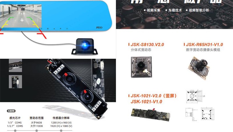
JSK Technology (Jinshikang) specializes in camera module OEM/ODM across consumer electronics, automotive, security, and industrial inspection, with multi-source CIS procurement (Sony plus Onsemi plus domestic), AA precision packaging, and automotive-grade reliability validation, helping overseas customers navigate the CIS architecture upgrade wave with sensor-agnostic design and selection-pitfall consulting, converging architectural decision risk into a single traceable node.
Stacked CIS carries a premium over same-resolution BSI due to the added logic-tier wafer and 3D integration process, with the exact uplift depending on process node and stack layers. Whether it is worth it depends on whether the application needs high-frame-rate multi-frame HDR, on-chip AI, or low power, automotive front-view and high-speed industrial inspection benefit clearly, while a fixed-focus surveillance camera may not.
As of September 2026, metasurface lenses are in mass production in consumer electronics (iPhone 17 Face ID, Xiaomi Civi 5 Pro), but the automotive-grade metasurface supply chain and AEC-Q certification framework are still maturing. Automotive projects should prioritize mature aspheric glass/plastic hybrid lenses, with metasurfaces tracked as R&D.
Event sensors suit scenarios needing microsecond latency and low-power continuous sensing, such as robotics pose capture and high-speed industrial inspection. Production risks include an algorithm ecosystem incompatible with traditional frame cameras, test standards (EMVA) not yet covering them, and mass-production yield still climbing, so small-batch validation before mass-production import is recommended.
AI-driven HBM and DRAM demand is tilting advanced wafer capacity toward memory, compressing stacked-CIS supply that depends on 28/22nm logic tiers. Buyers should lock capacity milestones rather than only price in contracts, sign long-term capacity reservations, and stock 8-inch-wafer smaller makers as a buffer.
In security and mid-tier automotive, domestic CIS can substitute; for high-end BSI stacked CIS, Sony should remain primary with domestic as second source. Before promoting domestic to primary, accumulate mass-production CPK data, confirm EMVA 1288 or other third-party certification, and adopt sensor-agnostic design to reduce changeover risk.


AR0230---1/2.7 HD 2M Wide Dynamic
Fatigue Monitoring Camera Module
Motion DV Camera-720P-120 Degree Wide Angle Camera Module
Night Vision Monitoring Camera Module
Monitoring - Doorbell - Law Enforcement Instrument Camera Module
Ten Thousand Trillion Industrial Camera Camera Module
 13423810014
 0755-29433686
 daming@cameras-module.com
 2/F, Building H, Zhiyihan Industrial Park, Yuanling Village, Shiyan Town, Baoan District, Shenzhen 518108



We use cookies to enhance your browsing experience. Continuing to browse indicates that you agree to our cookie policy.